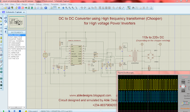
I posted this DC to DC
converter circuit for high voltage transformer-less inverter because of my
internet friend, Avila Pinto Joaquin of JAP/POWER ING who demanded for it. Its pure
sine wave transformer-less (TL)
inverter
section uses an advanced IGBT or MOSFET high power driver for high control
accuracy, high power factor and high efficiency with low harmonic.
The differences between standard or conventional inverters and transformer-less inverters are:
1. Conventional inverters are built with an internal bulky transformer that synchronizes the DC voltage with the AC output.
2. Transformer-less inverters uses a computerized multi-step process and electronic components to convert DC to high frequency AC, back to DC, and ultimately to standard-frequency AC.
3. Transformer-less inverters are light and compact. This means that it is much smaller and lighter in weight than inverters with bulky iron core transformers.
4. Transformer-less inverters have higher efficiency rating.
5. Transformer-less inverters use electronic switching rather than mechanical switching.
6. The amount of heat and humidity produced by standard inverters is greatly reduced using transformer-less method.
Using this DC to
DC converter circuit, a high efficient solar inverter can be achieved. The circuit
shown is a modified sine wave switching converter, which contains no bulky,
heavy and expensive iron transformer. It has advantage of being small in size and very light in weight. It has
precise output voltage stabilization and among other things, very little
quiescent power consumption, which cannot be achieved using the iron core
transformer. The chopper used in the design with the converter simulation is shown below:
High frequency chopper used in the circuit
Simulation of the DC to DC converter at 5.3Khz switching frequency,
Feel free to comment
and ask questions on the design. Information on how to add low voltage cutoff, overload
or short circuit protection can be discussed later based on demands.
WARNING
Be careful, the DC to DC converter circuit produces a very high voltage DC output that
can kill someone.
The inverter uses UC2525 or SG3525 which is designed for PWM switch mode power supply circuits. This circuit can also be implemented using micro-controller as shown in the pictures below:
Apart from using SG3524 or PIC16f716 micro-controller, other micro-controllers can be use. Study and follow the code below and use it. The code is for H- bridge inverter with pic in bult PWM controllers for generating sine wave inverter
// high frequency inverter code
#ifndef _XTAL_FREQ
#define _XTAL_FREQ 16000000
#define __delay_us(x) _delay((unsigned long)((x)*(_XTAL_FREQ/4000000.0)))
#define __delay_ms(x) _delay((unsigned long)((x)*(_XTAL_FREQ/4000.0)))
#endif
#include
__CONFIG(PROTECT&
HS& //INTIO& //internal
OSC_8MHZ&
WDTDIS&
MCLRDIS&
PWRTEN &
BOREN &
0x3FFF);
unsigned char sin_table[32] = {0, 25, 49, 73, 96, 118, 137,
159, 177, 193, 208, 220, 231, 239, 245, 249, 250, 249, 245,
239, 231, 220, 208, 193, 177, 159, 137, 118, 96, 73, 49, 25};
unsigned char index;
unsigned char soft_start_sh; //soft start shift count.
unsigned char soft_start_td; //soft start time delay.
unsigned int DUTY_CYCLE; //delay.
bit soft_start, wave_flag = 0;
void interrupt siva() {
if (TMR2IF == 1) {
TMR2IF = 0;
CCPR1L = 200; //sin_table[index];
// ++index;
if(index == 32)
{ index = 0;
wave_flag = ~wave_flag;
if( wave_flag) CCP1CON = 0x8D; //half bridge control
else CCP1CON = 0x8C; //half bridge control
}
}
}
void main() {
ANSEL = 0; //Disable ADC
CM1CON0 = 0; //Disable Comparator
CM2CON0 = 0; //Disable Comparator
VRCON = 0;
PR2 = 249; //16 khz@16MHZ
TRISC = 0x3F;
CCP1CON = 0x00;
ECCPAS = 0x40;
PWM1CON = 0x94; //5ussec
PRSEN = 1;
CCP1CON = 0x8D; //half bridge control
wave_flag = 0;
__delay_ms(500);
TMR2IF = 0;
T2CON = 0x24; //TMR2 on, prescaler and postscaler 1:5
while (TMR2IF == 0);
TMR2IF = 0;
TRISC = 0x03; //set pwm pins as o/p
TMR2IE = 1;
GIE = 1;
PEIE = 1;
RC2 = 0;
RC3 = 0;
while (1) {
if (ECCPASE) index = 0;
}
}
For the circuit
PWM 1A,1B,1C,1D pins form the H bridge circuit. IR2110 and IRF 740 MOSFETS are used for circuit. A
A waveform shown below can be gotten during the circuit simulation using the above source code.

A waveform shown below can be gotten during the circuit simulation using the above source code.

Feel free to make your suggestions, comments or ask questions: Call or Whatsapp +234-8037909203.
You can email us at: abledesigns@yahoo.com or engrable.ea@gmail.com if you want to buy any of our advanced schematic circuit diagrams, codes or products. Thanks and God bless.


